
Close Menu
geekfence.comgeekfence.com
    What's Hot

    The Best Backpacking Sleeping Pads, Tested on the Trail (2026)

    July 26, 2026

    AT&T bets its fiber and 600 MHz on agentic AI traffic

    July 26, 2026

    Stranded in the Slow Zone – O’Reilly

    July 26, 2026
    Facebook X (Twitter) Instagram
    • About Us
    • Contact Us
    Facebook Instagram
    geekfence.comgeekfence.com
    • Home
    • UK Tech News
    • AI
    • Big Data
    • Cyber Security
      • Cloud Computing
      • iOS Development
    • IoT
    • Mobile
    • Software
      • Software Development
      • Software Engineering
    • Technology
      • Green Technology
      • Nanotechnology
    • Telecom
    geekfence.comgeekfence.com
    Home»Nanotechnology»Tescan Unveils the New CLARA to Help Researchers See More at the Nanoscale
    Nanotechnology

    Tescan Unveils the New CLARA to Help Researchers See More at the Nanoscale

    AdminBy AdminJuly 26, 2026No Comments3 Mins Read1 Views
    Facebook Twitter Pinterest LinkedIn Telegram Tumblr Email
    Tescan Unveils the New CLARA to Help Researchers See More at the Nanoscale
    Share
    Facebook Twitter LinkedIn Pinterest Email


    Tescan has introduced the new generation of Tescan CLARA™, an ultra-high-resolution scanning electron microscope for nanoscale materials characterization. The system combines low-energy high-resolution SEM imaging, multi-contrast detection, support for challenging materials, and faster navigation from setup to results for research laboratories, shared microscopy facilities, and industrial R&D environments.
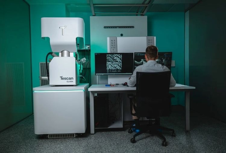
    Tescan Unveils the New CLARA to Help Researchers See More at the Nanoscale
    Image Credit: Tescan

    The new CLARA™ is intended for work in materials science, nanotechnology, advanced manufacturing, industrial R&D, and shared microscopy facilities. It supports imaging and analysis across a range of sample types, including polymers, magnetic materials, metals, ceramics, coatings, particles, and failure analysis samples.

    “In materials research, important information is often found in subtle surface structures, thin layers, local composition changes, or features that are difficult to image without changing the sample,” said Sirine Assaf, CRO at Tescan. “CLARA™ is designed to support this work by combining low-energy imaging, rich detection, and practical workflow control in one platform.”

    Clearer Nanoscale Imaging with Less Sample Preparation

    Many important material features can only be understood at the nanoscale. CLARA™ enables ultra-high-resolution imaging at low energy levels, which is especially valuable when working with delicate, non-conductive, or beam-sensitive samples.

    Low-energy imaging helps researchers observe fine surface structures while reducing the need for additional preparation steps such as conductive coating. This allows teams to study materials closer to their natural state and reduce the risk of preparation artifacts.

    For researchers studying nanoparticles, thin surface layers, coatings, contamination, or small defects, this combination of resolution and sample protection supports the interpretation of fine structural and material features.

    More Insight From Every Measurement

    CLARA™ is designed to collect complementary types of information from the same area of a sample, helping researchers distinguish surface detail from material differences.

    This multi-contrast approach can help identify near-surface particles, contamination layers, composition changes, or material variations that may be difficult to separate from topographic contrast alone.

    Analytical Flexibility for Research and Industrial Laboratories

    Modern research and industrial laboratories rarely work with one simple sample type. One day may involve a conductive metal, the next a polymer, magnetic material, porous structure, coating, fracture surface, or sensitive prototype component.

    CLARA™ supports high-resolution SEM imaging across challenging materials and offers low-vacuum capability for samples that charge, outgas, or require gentler imaging conditions. Researchers can adapt imaging conditions to the sample rather than forcing the sample into a fixed workflow.

    The system also supports a range of analytical techniques, enabling laboratories to connect high-resolution imaging with deeper material analysis. CLARA™ is suited to applications in advanced materials research, electronics, energy materials, metallurgy, polymers, coatings, nanotechnology, failure analysis, and quality control.

    With CLARA™, Tescan continues to develop electron microscopy solutions that combine performance, usability, and analytical flexibility for routine and advanced nanoscale characterization.


    Source link

    Share. Facebook Twitter Pinterest LinkedIn Tumblr Email

    Related Posts

    New programmable photonic chip can control how fast light moves

    July 25, 2026

    Immunostimulatory lipogel implant enhances cancer immunotherapy

    July 23, 2026

    The physics of protein condensates – Physics World

    July 22, 2026

    Invisible Microbes ‘Mining’ Toxic Waste in the Flinders Ranges

    July 21, 2026

    A tiny universe in a bottle reveals clues to the origins of life

    July 20, 2026

    The simplicity of a twist

    July 18, 2026
    Top Posts

    Understanding U-Net Architecture in Deep Learning

    November 25, 202566 Views

    Hard-braking events as indicators of road segment crash risk

    January 14, 202633 Views

    Redefining AI efficiency with extreme compression

    March 25, 202631 Views
    Don't Miss

    The Best Backpacking Sleeping Pads, Tested on the Trail (2026)

    July 26, 2026

    I’ve had very few problems with any inflatable sleeping pad I’ve tested. Some have lost…

    AT&T bets its fiber and 600 MHz on agentic AI traffic

    July 26, 2026

    Stranded in the Slow Zone – O’Reilly

    July 26, 2026

    Data Science Case Study: The SCOPE Framework Guide

    July 26, 2026
    Stay In Touch
    • Facebook
    • Instagram
    About Us

    At GeekFence, we are a team of tech-enthusiasts, industry watchers and content creators who believe that technology isn’t just about gadgets—it’s about how innovation transforms our lives, work and society. We’ve come together to build a place where readers, thinkers and industry insiders can converge to explore what’s next in tech.

    Our Picks

    The Best Backpacking Sleeping Pads, Tested on the Trail (2026)

    July 26, 2026

    AT&T bets its fiber and 600 MHz on agentic AI traffic

    July 26, 2026

    Subscribe to Updates

    Please enable JavaScript in your browser to complete this form.
    Loading
    • About Us
    • Contact Us
    • Disclaimer
    • Privacy Policy
    • Terms and Conditions
    © 2026 Geekfence.All Rigt Reserved.

    Type above and press Enter to search. Press Esc to cancel.